Non-Contact Measurement Supports Growth in Consumer Electronics Market
The demand for touchscreen technology remains strong, but the supply chain continues to tighten as 2026 unfolds. Business Research Insights notes that the touchscreen module — the integrated, layered touch-sensitive component in devices — is projected to be USD $46.07 billion in 2026,with a CAGR of 34.81% until 2035.
However, recent market data from Counterpoint Research shows that global smartphone shipments are now projected to decline by about 2.1% in 2026, driven largely by surging memory and component costs that continue to strain manufacturers.
Two other market constraints placing downward pressure on production capabilities for smartphones include:
- Poor accuracy in the quality assurance process, leading to reduced throughput and output.
- Consumer expectations for quality assurance and durability continue to climb as OLED gains share in smartphones and LCD remains common in tablets, monitors, and value‑tier phones. Consistent layer‑stack uniformityis crucial to performance and reliability
As such, manufacturers face mounting pressure to ensure that the layer stacks are uniform. This makes reducing any production deficiencies key to both the ability to meet market demand and satisfaction. An important development to support this goal is the use of white light interferometry to perform highly accurate non-contact thickness measurements.
Layers Within Touchscreens
Historically, touchscreens for tablets, smartphones, and computers generally consist of two independent modules: the imaging display and the touch module, with the latter placed on top of the display. The imaging display creates the image, while the touch module allows the user to interact with the device.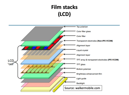
Other modern devices use integrated in‑cell/on‑cell sensors that re built directly into the display stack, reducing thickness, improving optical clarity, and simplifying lamination compared to traditional modules.
The most commonly used type of imaging display is the liquid‐crystal display or LCD. The light from a backlight source is distributed throughout the screen by a layer of a diffuser (a light guide with a brightness enhancement film). The light then passes the first polarizer and travels through a layer containing liquid crystals sandwiched between two layers of electrodes. The liquid crystals are activated by the electric signal. In the case of the active matrix display, the bottom electrode layer consists of an array of thin‐film‐transistors located on a substrate.
Another widely used imaging display technology is the organic light‑emitting diode or OLED display. Unlike LCDs, OLEDs are self‑emissive, meaning each pixel generates its own light without the need for a backlight. An OLED panel is constructed from multiple ultra‑thin organic material layers deposited onto a substrate. These layers are sandwiched between two electrodes: a cathode and an anode. When an electric current is applied, electrons and holes recombine within the organic emissive layer, producing light directly at the pixel level.
How Can You Boost Production Levels?
The OptiGauge II and OptiGauge II-EMS help increase production throughputs and reduces costs associated with consumer electronics manufacturing.

Similar to imaging displays, there are a variety of touchscreen technologies on the market. The most common touchscreen technology is capacitive, which is based on detecting the change in the capacitance between two arrays of electrodes when the human finger approaches the surface of the screen.
The different components of these displays and touchscreens must be consolidated into one unit. This is done by manufacturers using a layer of adhesive, the uniformity of which can be difficult to control during the production process.
The Role of Low‐Coherence Interferometry
To control the thickness of the adhesive layer during the manufacturing process, the manufacturer must be able to measure the thickness of the layer during or after the manufacturing process. Optical non-destructive measurement addresses this by allowing 100% inspection, on‐ or at‐line, in real-time. This is the ideal application of low‐coherence interferometry.
The light from a low‐coherence light source is split into two portions. These two portions form sample and reference interferometric arms. The sample portion of the light illuminates the layer stack of a touchscreen or some other device. Each surface within the layer stack reflects the incident light. The reflected light is then combined with the reference portion of the light. The combined light creates an interferometric pattern.
However, in the case of the low-coherence light source, the interferometric pattern is visible only under certain conditions, when the path traveled by the light in the sample arm of the interferometer (to and from the corresponding sample interface) is equal to the path in the reference arm of the interferometer.
By varying the length of the reference arm of the interferometer, and by measuring the magnitude of the change between the locations where the interferometric pattern appears, one can extract the distances between the reflective interfaces within the sample, i.e. the layer thicknesses.
What are the benefits of using Lumetrics' non-contact measurement solutions?
Using this non-contact measurement technology, the layer thicknesses in the touchscreens can be
measured within a continuous scan, instead of at a single point. To obtain thickness variation along with the scan, the screen (or the optical probe) is moved along the predetermined path, while the thickness of the layers is being continuously measured. This scan identifies significant inconsistencies in the manufacturing process that cannot be seen with a naked eye, and cannot be directly measured by any mechanical means.
Low‐coherence interferometry instruments provide a clear advantage over mechanical measurement methods as discussed above. Lumetrics’ commercially available OptiGauge II serves as a comprehensive, practical tool for non‐destructive product metrology and quality control during and after the manufacturing process which enables manufacturers of consumer electronics and their components to increase production, reduce waste, and ultimately, meet the demand to maximize their growth.
To learn more, download the Lumetrics whitepaper:
Measurement of Film Stacks in Cell Phones and Tablets Using White Light Interferometry.

Need help maximizing your production output? Talk to an engineer to see how interferometry can work for you.