By Dave Compertore, Scientist, Lumetrics®, Inc.
Over the past several years, shortages of semiconductors and the components used to make them, such as raw silicon, have had heavy repercussions for manufacturers of chip-based products in the automotive, high tech, and military market sectors.
The cause of these shortages can be attributed to the trickle-down effect of a silicon wafer shortage which is limiting the production of microprocessor chips—a trend that continues to impact semiconductor manufacturers.
To meet the increasing demand for semiconductors under the current constraints of decreased supply of silicon, which is used to produce wafers—an integral product component—semiconductor manufacturers must be strategic in their approach to fabrication.
Complexities of Semiconductor Manufacturing
| 65+ Pieces of equipment required to make one wafer |
$28 Billion Estimated spend on new plants & equipment by a single major manufacturer |
5 Nanometers dimensions of today's processor node |
Source: Bloomberg.com
The key is to implement quality control mechanisms that allow semiconductor production facilities to maximize output and minimize waste. Reducing costly quality issues and implementing the best possible quality assurance processes (like defect inspection) can avoid the loss of entire batches of silicon wafer chips.
How Interferometry May Increase Quality Throughput
The non-contact measurement of silicon wafers is critical for ensuring accurate thickness of these components. Defining and obtaining accurate thickness measurements are essential for reducing anomalies in patterning and packaging problems during semiconductor fabrication.
Accurately measuring semiconductor chips early in the manufacturing process allows product engineers, quality managers, plant managers, and lab managers to identify product issues as soon as possible and make alterations to reduce the costs associated with silicon waste, reduced output, and defective products while maximizing throughput to meet market demand and support related revenue targets.
Low coherence interferometers improve and sustain the precision of polished silicon wafers throughout the production process. Interferometry can quickly discern unintended thickness pattern changes in wafers or layers added to wafers. These patterns can then be measured and analyzed to ensure they are within the specifications of the manufacturing process.
Interferometry devices are often used in automotive and high-tech applications with products that feature larger silicon wafer chips such as hermetic packages, protective seals, and other products such as those related to directionality in vehicles. The ultimate goal of incorporating the higher level of accuracy in these manufacturing processes that non-contact thickness measurement provides is to obtain improvements in facility yields.
A Deeper Look at Silicon Wafer MeasurementOur newest app note explores how the Lumetrics OptiGauge II measures the simultaneous wafer thickness, adhesive thickness, and parallelism between surfaces to sub-micron precision
|

Integrating Non-contact Interferometry to Maximize Semiconductor Production Yields
The use of interferometric devices allows semiconductor manufacturers to assess exceedingly small measurements that are outside the capabilities of other measurement methodologies. For example, a unique capability of the OptiGauge II is its ability to measure the individual layer thickness of a multiple layer sample using a 1310 nm wavelength. This is an ideal wavelength for measuring through all visually transparent and semitransparent objects which can scan thicknesses of extremely thin wafers down to 2/10 of a micron.
Interferometric devices can also be seamlessly integrated within existing semiconductor production workflows to augment the measurements of precision XY scanners or robotic systems. The addition of this type of non-contact thickness measurement in the semiconductor production process provides the opportunity for quality assurance teams to pivot quickly in the case of non-conforming product components being flagged in the production line. By precisely measuring the wafer and maintaining the correct thickness (within 0.1 of a micron for wafer specifications) and width of the silicon chip, the ultimate goal of thickness uniformity can be achieved which would not be possible using traditional measurement protocols.
Reduce the Impact of Silicon Chip Shortages on your Semiconductor Production Workflows
With high levels of precision measurements in hand, fabricators have the potential to reduce waste associated with lack of adherence to manufacturing specifications and reduce the cost of production accordingly. This scenario also creates a more efficient workflow with less downtime and more throughput given the increased accuracy of the production process in general.
Interferometric devices like the OptiGauge II are proven in the MEMS fabrication process. Figure 1 demonstrates the capability of the OptiGauge II to scan a patterned 3 mm by 3 mm Si wafer at 50 µm x 50 µm resolution. The vertical axis represents the wafer thickness. The roughness is on the order of a few µm, with several multiple µm “holes” scattered about.
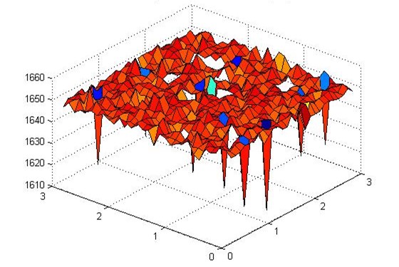
Figure 1: Surface roughness and “holes” in a patterned silicon wafer, modeled by the OptiGauge II
Figure 2 is an example of how the OptiGauge Control Center, the software interface of the OptiGauge II, appears during the measurement of the MEMS sample. A peak represents an interface between layers. The distance between two peaks equals the optical thickness (OT) of the material. The refractive index (RI) of the material is then used to convert the optical thickness to a physical thickness (T) using this equation: T=OT/RI
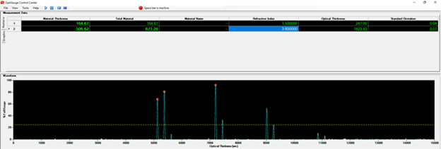
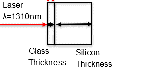
Figure 2: The OptiGauge interface clearly shows peaks of interference from the scan in Figure 1.
Note: Figures 1 and 2 are for demonstration purposes only. The data assumes a refractive index of 1.5 for the material of the glass, and 3.6 for the silicon.
Similar to the MEMS example, interferometric instruments can provide semiconductor fabricators with precision measurements to help reduce the fallout of an already critically low supply of raw silicon, thereby mitigating the downward pressure on production capabilities that it causes.
If you need help maximizing your production output, talk to an engineer to see HOW interferometry can work for you.