

Non-Contact Wafer Inspection & Measurement
Wafer Thickness Measurement & Inspection for Silicon Wafers
Lumetrics provides wafer thickness measurement systems for semiconductor and advanced materials that need accurate, non-contact inspection. Using Low-Coherence Interferometry technology, our systems help measure wafer thickness, detect voids in bonded assemblies, and evaluate flatness or bow without damaging the part. In this video, Lumetrics Metrology Scientist, Dr. Paul Thomas, Ph.D., provides insights on how Lumetrics non-contact optical metrology technology can be used for this application.
Dr. Thomas utilizes the Lumetrics OptiGauge II to demonstrate thickness measurements on a bare silicon wafer and to detect voids on the wafer that has been bonded to glass. The Lumetrics OptiGauge II system is flexible, and can also be configured in such a manner making it simple to determine flatness or bow.
Take a look at our wafer measurement use cases to learn how the OptiGauge II may help you address your semiconductor measurement and inspection challenges.
Why Wafer Measurements Requires a Non-Contact Approach
Silicon wafers and bonded wafer assemblies demand precise measurement without introducing handing damage, contamination, or inconsistent results. As wafer processes become more specialized, teams need inspection tools that can support thickness verification, bonded-interface evaluation, and geometry checks within the same broader workflow.
Traditional contact methods can be limiting when the job also includes void detection, delicate surfaces, or advanced bonded structures. Lumetrics helps solve that problem with optical metrology designed for repeatable, non-destructive inspection.
Wafer Measurement Use Cases
Lumetrics systems support wafer inspection applications such as:
- Bare silicon wafer thickness measurement
- Bonded silicon-to-glass void detection
- Flatness and bow evaluation
- Process development and engineering analysis
- Quality Inspection for advanced wafer assemblies
Typical Applications
Built for Semiconductor and Advanced Materials
Lumetrics systems are used by teams that need practical inspection tools for R&D, quality, and production workflows. The goal is to make wafer measurement faster, more repeatable, and more useful for engineering decisions, without forcing destructive sample prep.
Featured Products & Systems
- OptiGauge II
- OptiGauge 600
- Shack-Hartmann Wavefront Sensor
The OptiGauge II is an ideal non-contact thickness gauge for companies needing an accurate, non-contact system for single and multilayer thickness measurement. The OptiGauge II can measure multilayer glass, PVB, acoustic PVB, and can determine wedge angle of automotive glass.

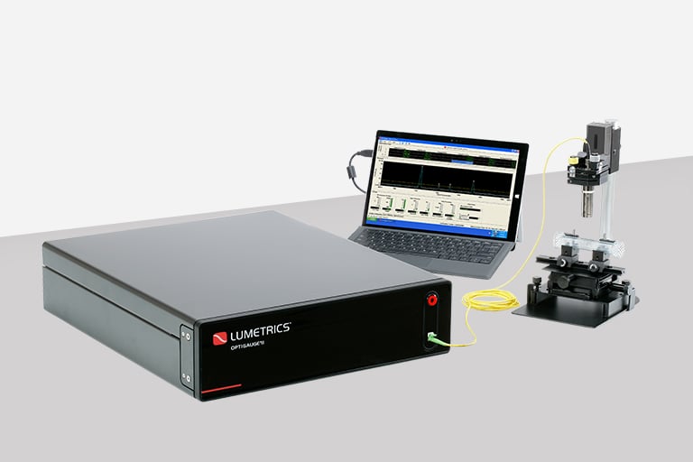
The OG-600 uses visible light with the center wavelength of approximately 650 nm and is designed to measure windshields with or without IR coating.

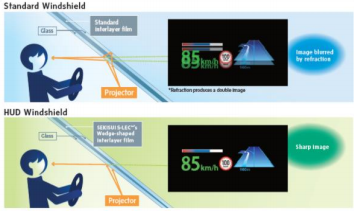
The windshield has become an increasingly complex component of an automobile requiring the latest metrology tools to meet the demands of the world’s leading automotive manufacturers. The Shack-Hartmann Wavefront Sensor from Lumetrics is used to determine optical distortion of a windshield and calculate wedge angle.

Silicon Wafer Resources
Review wafer-focused technical material to see how Lumetrics systems are used for thickness, flatness, and bonded-wafer inspection challenges.


