 Abstract—The silicon wafer manufacturing process relies heavily on precision polished wafers that have uniform thickness and, depending on the application, also control parallelism to a secondary wafer after bonding.
Lumetrics’ low coherence interferometer, commercially marketed as OptiGauge II, is a device capable of measuring the simultaneous wafer thickness, adhesive thickness, and parallelism between surfaces to sub-micron precision. Combined with custom software and a precision XY raster scanner, a wafer or wafer assembly can be fully characterized with respect to layer thicknesses and surface parallelism.
Index Terms—adhesive, flatness, interferometry, metrology, optical thickness measurement, parallelism, silicon, wafer
I. Introduction:
Lumetrics is the market leader in providing high-precision, non-contact optical thickness measurements to medical, scientific, and ophthalmic industries.
A unique capability of our flagship thickness measurement device, OptiGauge II, is its ability to measure the individual layer thickness of a multiple-layer sample.
The OptiGauge II measures using a 1310nm wavelength. This is an ideal wavelength for measuring through nearly all visually transparent and semi-transparent objects.
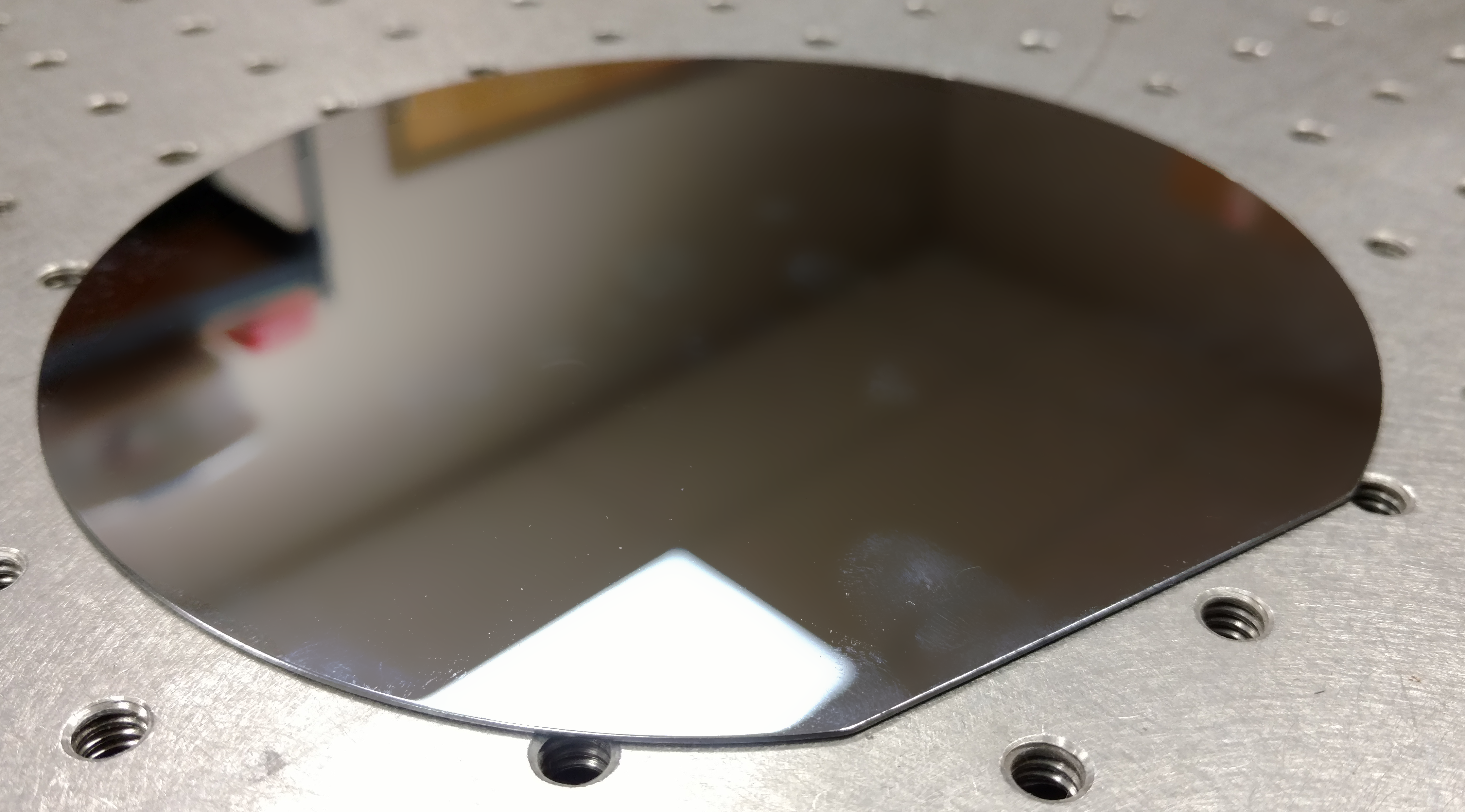
A visually opaque material that is highly transmissive at 1310nm is silicon. This makes silicon an ideal sample for optical thickness measurement.